
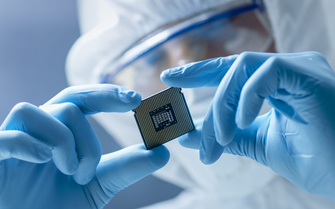
The NTU researchers and their colleagues from the Korean Institute of Mechanical Engineering and Materials (KIMM) have developed a chemical-free printing technique, which, when combined with metal-assisted chemical etching, results in semiconductor wafers with nanowires – nanostructures in cylindrical form – that are highly uniform and scalable. These semiconductors, described in the journal ACS Nano, also demonstrated better performance when compared to current chips in the market.
The nanotransfer printing technique is accomplished by transferring gold nanostructure layers onto a silicon substrate at a low temperature of 160 °C to form a highly uniform plate with nanowires that can be controlled to the desired thickness during production. In laboratory tests, the researchers were able to achieve more than 99 percent yield transfer of a 20-nanometer-thick gold film onto a 15-centimeter silicon wafer. The research team believes the same technique can be applied to wafers twice this size (30 cm or 12 inch), which is the mainstream wafer size in the current production lines of semiconductor chipmakers like Samsung, Intel, and GlobalFoundries.
As the COVID-19 pandemic slowed supply routes, manufacturers from a number of industries, especially carmakers and telecommunications businesses, had to reduce production volumes and slow deliveries to customers. But now it seems that the problem could be overcome with the help of the new printing technology.
Semiconductor chips are usually fabricated on silicon and then diced into the small chips that are used in devices. However, the process is imperfect, so defective chips are discarded, which in turn increases production cost. Nanotransfer-based printing – a process that uses a polymer mold to print metal onto a substrate through pressure, or ‘stamping’ – is simpler, more cost-effective, and has high throughput. The problem is that nanotechnology uses a chemical adhesive layer that causes negative effects such as surface defects and performance degradation when printed on a large scale and is hazardous to human health. The new chemical-free production method eliminates this risk.
The problem with the shortage of chips is particularly pronounced in Europe, so Intel recently announced its expansion in the regional semiconductor market with an investment cycle of as much as €80 billion. The cycle will last up to ten years, and the plan includes the entire supply chain, from research and development, through chip production, to the development of new packaging technologies. As much as €17 billion will be invested in a modern chip plant in Germany, which will employ about 3,000 people, in addition to an R&D lab in France, and foundries and other plants in Ireland, Italy, Poland and Spain. New investments in Ireland will reach €12 billion, and in Italy €4.5 billion, along with the creation of tens of thousands of jobs, both in Intel and their closely related suppliers.
The investments are in line with the European Green Deal, as well as with the recently adopted European Chips Act, so it is clear that the EU will participate in this investment to some extent.
